
Reference: RBD-1354
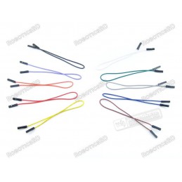
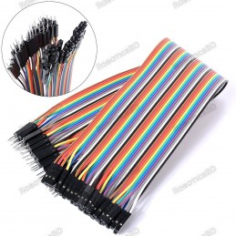
Jumper Wire Single 20cm
Length: 8 inches/20 CM (Long) Material: Copper Plated Pin Spacing: 2.54mm.
Reference: RBD-1354
Length: 8 inches/20 CM (Long) Material: Copper Plated Pin Spacing: 2.54mm.
Reference: 0245
Choose your desire Resistor value from below:
Reference: RBD-0351
Contactless transmission of data and supply energy (no battery needed) Operating distance: Up to 100mm (depending on antenna geometry) RoboticsBD Operating frequency: 13.56MHz Data transfer: 106 kbit/s Data integrity: 16 Bit CRC, parity, bit coding bit counting Anticollision Typical ticketing transaction: <100 ms ( including backup management)...
Reference: 0031
3 Types Available (Please select from option) 1. Male to Male 2. Male to Female 3. Female-Female
Reference: RBD-0768
Size: 5mm Color: RED Head Shape: Round Lens Appearance: Transparent
Reference: RBD-0761
Breadboard friendly Mounting Style: Through Hole Mounting Direction: Vertical
Reference: RBD-0094
The Arduino Uno R3 High-Quality Edition Arduino UNO in Bangladesh Micro-controller : ATmega328. Operating Voltage : 5V. Input Voltage (recommended) : 7-12V. Digital I/O Pins : 14 (of which 6 provide PWM output). Analog Input Pins : 6. The Arduino Uno R3 High-Quality Edition embodies superior craftsmanship and meticulous attention to detail, resulting in...
Call For Price
01783 007 004
Omron CJ1W-OD202
Name | 8-point DC Input Unit with Terminal Block |
---|---|
Model | CJ1W-ID201 |
Rated Input Voltage | 12 to 24 VDC |
Rated Input Voltage Range | 10.2 to 26.4 VDC |
Input Impedance | 2.4 kΩ |
Input Current | 10 mA typical (at 24 VDC) |
ON Voltage/ON Current | 8.8 VDC min./3 mA min. |
OFF Voltage/OFF Current | 3 VDC max./1 mA max. |
ON Response Time | 8.0 ms max. (Can be set to between 0 and 32 ms in the Setup.) *1 |
OFF Response Time | 8.0 ms max. (Can be set to between 0 and 32 ms in the Setup.) *1 |
Number of Circuits | 8 independent circuits |
Number of Simultaneously ON Points |
100% simultaneously ON |
Insulation Resistance | 20 MΩ min. between external terminals and the GR terminal (100 VDC) |
Dielectric Strength | 1,000 VAC between the external terminals and the GR terminal for 1 minute at a leakage current of 10 mA max. |
Internal Current Consumption | 80 mA max. |
Weight | 110 g max. |
Circuit Configuration |
![]() The signal names of the terminals are the device variable names. The device variable names are the names that use "Jxx" as the device name. |
External connection and terminal-device variable diagram |
![]() Polarity of the input power supply can be connected in either direction. The signal names of the terminals are the device variable names. The device variable names are the names that use "Jxx" as the device name. |
Name | 16-point DC Input Unit with Terminal Block | |
---|---|---|
Model | CJ1W-ID211 | |
Rated Input Voltage | 24 VDC | |
Rated Input Voltage Range | 20.4 to 26.4 VDC | |
Input Impedance | 3.3 kΩ | |
Input Current | 7 mA typical (at 24 VDC) | |
ON Voltage/ON Current | 14.4 VDC min./3 mA min. | |
OFF Voltage/OFF Current | 5 VDC max./1 mA max. | |
ON Response Time | 8.0 ms max. (Can be set to between 0 and 32 ms in the Setup.) *1 | |
OFF Response Time | 8.0 ms max. (Can be set to between 0 and 32 ms in the Setup.) *1 | |
Number of Circuits | 16 (16 points/common, 1 circuit) | |
Number of Simultaneously ON Points |
100% simultaneously ON (at 24 VDC) (Refer to the following illustration.) | |
Insulation Resistance | 20 MΩ min. between external terminals and the GR terminal (100 VDC) | |
Dielectric Strength | 1,000 VAC between the external terminals and the GR terminal for 1 minute at a leakage current of 10 mA max. |
|
Internal Current Consumption | 80 mA max. | |
Weight | 110 g max. | |
Circuit Configuration |
![]() The signal names of the terminals are the device variable names. The device variable names are the names that use "Jxx" as the device name. |
![]() |
External connection and terminal-device variable diagram |
![]() Polarity of the input power supply can be connected in either direction. The signal names of the terminals are the device variable names. The device variable names are the names that use "Jxx" as the device name. |
Name | 16-point DC Input Unit with Terminal Block | |
---|---|---|
Model | CJ1W-ID212 | |
Rated Input Voltage | 24 VDC | |
Rated Input Voltage Range | 20.4 to 26.4 VDC | |
Input Impedance | 3.3 kΩ | |
Input Current | 7 mA typical (at 24 VDC) | |
ON Voltage/ON Current | 14.4 VDC min./3 mA min. | |
OFF Voltage/OFF Current | 5 VDC max./1 mA max. | |
ON Response Time | 8.0 ms max. (Can be set to between 0 and 32 ms in the Setup.) *1 | |
OFF Response Time | 8.0 ms max. (Can be set to between 0 and 32 ms in the Setup.) *1 | |
Number of Circuits | 16 (16 points/common, 1 circuit) | |
Number of Simultaneously ON Points |
100% simultaneously ON (at 24 VDC) (Refer to the following illustration.) | |
Insulation Resistance | 20 MΩ min. between external terminals and the GR terminal (100 VDC) | |
Dielectric Strength | 1,000 VAC between the external terminals and the GR terminal for 1 minute at a leakage current of 10 mA max. |
|
Internal Current Consumption | 130 mA max. | |
Weight | 110 g max. | |
Circuit Configuration |
![]() The signal names of the terminals are the device variable names. The device variable names are the names that use "Jxx" as the device name. |
![]() |
External connection and terminal-device variable diagram |
![]() Polarity of the input power supply can be connected in either direction. The signal names of the terminals are the device variable names. The device variable names are the names that use "Jxx" as the device name. |
Name | 32-point DC Input Unit with Fujitsu Connector | |
---|---|---|
Model | CJ1W-ID231 | |
Rated Input Voltage | 24 VDC | |
Rated Input Voltage Range | 20.4 to 26.4 VDC | |
Input Impedance | 5.6 kΩ | |
Input Current | 4.1 mA typical (at 24 VDC) | |
ON Voltage/ON Current | 19.0 VDC min./3 mA min. | |
OFF Voltage/OFF Current | 5 VDC max./1 mA max. | |
ON Response Time | 8.0 ms max. (Can be set to between 0 and 32 in the Setup.) * | |
OFF Response Time | 8.0 ms max. (Can be set to between 0 and 32 in the Setup.) * | |
Number of Circuits | 32 (16 points/common, 2 circuits) | |
Number of Simultaneously ON Points |
75% (12 points/common) simultaneously ON (at 24 VDC) (Refer to the following illustration.) | |
Insulation Resistance | 20 MΩ min. between external terminals and the GR terminal (100 VDC) | |
Dielectric Strength | 1,000 VAC between the external terminals and the GR terminal for 1 minute at a leakage current of 10 mA max. |
|
Internal Current Consumption | 90 mA max. | |
Weight | 70 g max. | |
Accessories | None | |
Circuit Configuration |
![]() The signal names of the terminals are the device variable names. The device variable names are the names that use "Jxx" as the device name. |
![]() |
External connection and terminal-device variable diagram |
![]() The input power polarity can be connected in either direction. Be sure to wire both pins A9 and A18 (COM0), and set the same polarity for both pins. Be sure to wire both pins B9 and B18 (COM1), and set the same polarity for both pins. The signal names of the terminals are the device variable names. The device variable names are the names that use "Jxx" as the device name. |
Name | 32-point DC Input Unit with MIL Connector | |
---|---|---|
Model | CJ1W-ID232 | |
Rated Input Voltage | 24 VDC | |
Rated Input Voltage Range | 20.4 to 26.4 VDC | |
Input Impedance | 5.6 kΩ | |
Input Current | 4.1 mA typical (at 24 VDC) | |
ON Voltage/ON Current | 19.0 VDC min./3 mA min. | |
OFF Voltage/OFF Current | 5 VDC max./1 mA max. | |
ON Response Time | 8.0 ms max. (Can be set to between 0 and 32 in the Setup.) * | |
OFF Response Time | 8.0 ms max. (Can be set to between 0 and 32 in the Setup.) * | |
Number of Circuits | 32 (16 points/common, 2 circuits) | |
Number of Simultaneously ON Points |
75% (12 points/common) simultaneously ON (at 24 VDC) (Refer to the following illustration.) | |
Insulation Resistance | 20 MΩ min. between external terminals and the GR terminal (100 VDC) | |
Dielectric Strength | 1,000 VAC between the external terminals and the GR terminal for 1 minute at a leakage current of 10 mA max. |
|
Internal Current Consumption | 90 mA max. | |
Weight | 70 g max. | |
Accessories | None | |
Circuit Configuration |
![]() The signal names of the terminals are the device variable names. The device variable names are the names that use "Jxx" as the device name. |
![]() |
External connection and terminal-device variable diagram |
![]() The input power polarity can be connected in either direction. Be sure to wire both pins 23 and 24 (COM0), and set the same polarity for both pins. Be sure to wire both pins 3 and 4 (COM1), and set the same polarity for both pins. The signal names of the terminals are the device variable names. The device variable names are the names that use "Jxx" as the device name. |
Name | 32-point DC Input Unit with MIL Connector | |
---|---|---|
Model | CJ1W-ID233 | |
Rated Input Voltage | 24 VDC | |
Rated Input Voltage Range | 20.4 to 26.4 VDC | |
Input Impedance | 5.6 kΩ | |
Input Current | 4.1 mA typical (at 24 VDC) | |
ON Voltage/ON Current | 19.0 VDC min./3 mA min. | |
OFF Voltage/OFF Current | 5 VDC max./1 mA max. | |
ON Response Time | 8.0 ms max. (Can be set to between 0 and 32 in the Setup.) * | |
OFF Response Time | 8.0 ms max. (Can be set to between 0 and 32 in the Setup.) * | |
Number of Circuits | 32 (16 points/common, 2 circuits) | |
Number of Simultaneously ON Points |
75% (12 points/common) simultaneously ON (at 24 VDC) (Refer to the following illustration.) | |
Insulation Resistance | 20 MΩ min. between external terminals and the GR terminal (100 VDC) | |
Dielectric Strength | 1,000 VAC between the external terminals and the GR terminal for 1 minute at a leakage current of 10 mA max. |
|
Internal Current Consumption | 200 mA max. | |
Weight | 70 g max. | |
Accessories | None | |
Circuit Configuration |
![]() The signal names of the terminals are the device variable names. The device variable names are the names that use "Jxx" as the device name. |
![]() |
External connection and terminal-device variable diagram |
![]() The input power polarity can be connected in either direction. Be sure to wire both pins 23 and 24 (COM0), and set the same polarity for both pins. Be sure to wire both pins 3 and 4 (COM1), and set the same polarity for both pins. The signal names of the terminals are the device variable names. The device variable names are the names that use "Jxx" as the device name. |
Name | 64-point DC Input Unit with Fujitsu Connector | |
---|---|---|
Model | CJ1W-ID261 | |
Rated Input Voltage | 24 VDC | |
Rated Input Voltage Range | 20.4 to 26.4 VDC | |
Input Impedance | 5.6 kΩ | |
Input Current | 4.1 mA typical (at 24 VDC) | |
ON Voltage/ON Current | 19.0 VDC min./3 mA min. | |
OFF Voltage/OFF Current | 5 VDC max./1 mA max. | |
ON Response Time | 8.0 ms max. (Can be set to between 0 and 32 in the Setup.) * | |
OFF Response Time | 8.0 ms max. (Can be set to between 0 and 32 in the Setup.) * | |
Number of Circuits | 64 (16 points/common, 4 circuits) | |
Number of Simultaneously ON Points |
50% (16 points/common) simultaneously ON (at 24 VDC) (Refer to the following illustrations.) | |
Insulation Resistance | 20 MΩ min. between external terminals and the GR terminal (100 VDC) | |
Dielectric Strength | 1,000 VAC between the external terminals and the GR terminal for 1 minute at a leakage current of 10 mA max. |
|
Internal Current Consumption | 90 mA max. | |
Weight | 110 g max. | |
Accessories | None | |
Circuit Configuration |
![]() The signal names of the terminals are the device variable names. The device variable names are the names that use "Jxx" as the device name. |
![]() |
External connection and terminal-device variable diagram |
CN1 | CN2 |
![]() The input power polarity can be connected in either direction. Be sure to wire both pins A9 and A18 (COM0) of CN1, and set the same polarity for both pins. Be sure to wire both pins B9 and B18 (COM1) of CN1, and set the same polarity for both pins. The signal names of the terminals are the device variable names. The device variable names are the names that use "Jxx" as the device name. |
![]() The input power polarity can be connected in either direction. Be sure to wire both pins A9 and A18 (COM2) of CN2, and set the same polarity for both pins. Be sure to wire both pins B9 and B18 (COM3) of CN2, and set the same polarity for both pins. The signal names of the terminals are the device variable names. The device variable names are the names that use "Jxx" as the device name. |
Name | 64-point DC Input Unit with MIL Connector | |
---|---|---|
Model | CJ1W-ID262 | |
Rated Input Voltage | 24 VDC | |
Rated Input Voltage Range | 20.4 to 26.4 VDC | |
Input Impedance | 5.6 kΩ | |
Input Current | 4.1 mA typical (at 24 VDC) | |
ON Voltage/ON Current | 19.0 VDC min./3 mA min. | |
OFF Voltage/OFF Current | 5 VDC max./1 mA max. | |
ON Response Time | 8.0 ms max. (Can be set to between 0 and 32 in the Setup.) * | |
OFF Response Time | 8.0 ms max. (Can be set to between 0 and 32 in the Setup.) * | |
Number of Circuits | 64 (16 points/common, 4 circuits) | |
Number of Simultaneously ON Points |
50% (8 points/common) simultaneously ON (at 24 VDC) (Refer to the following illustrations.) | |
Insulation Resistance | 20 MΩ min. between external terminals and the GR terminal (100 VDC) | |
Dielectric Strength | 1,000 VAC between the external terminals and the GR terminal for 1 minute at a leakage current of 10 mA max. |
|
Internal Current Consumption | 90 mA max. | |
Weight | 110 g max. | |
Accessories | None | |
Circuit Configuration |
![]() The signal names of the terminals are the device variable names. The device variable names are the names that use "Jxx" as the device name. |
![]() |
External connection and terminal-device variable diagram |
CN1 | CN2 |
![]() The input power polarity can be connected in either direction. Be sure to wire both pins 23 and 24 (COM0) of CN1, and set the same polarity for both pins. Be sure to wire both pins 3 and 4 (COM1) of CN1, and set the same polarity for both pins. The signal names of the terminals are the device variable names. The device variable names are the names that use "Jxx" as the device name. |
![]() The input power polarity can be connected in either direction. Be sure to wire both pins 23 and 24 (COM2) of CN2, and set the same polarity for both pins. Be sure to wire both pins 3 and 4 (COM3) of CN2, and set the same polarity for both pins. The signal names of the terminals are the device variable names. The device variable names are the names that use "Jxx" as the device name. |
Name | 8-point AC Input Unit with Terminal Block |
---|---|
Model | CJ1W-IA201 |
Rated Input Voltage | 200 to 240 VAC 50/60 Hz |
Rated Input Voltage Range | 170 to 264 VAC |
Input Impedance | 21 kΩ (50 Hz), 18 kΩ (60 Hz) |
Input Current | 9 mA typical (at 200 VAC, 50 Hz), 11 mA typical (at 200 VAC, 60 Hz) |
ON Voltage/ON Current | 120 VAC min./4 mA min. |
OFF Voltage/OFF Current | 40 VAC max./2 mA max. |
ON Response Time | 18.0 ms max. (default setting: 8 ms) *1 |
OFF Response Time | 48.0 ms max. (default setting: 8 ms) *1 |
Number of Circuits | 8 (8 points/common, 1 circuit) |
Number of Simultaneously ON Points |
100% (8 points/common) simultaneously ON |
Insulation Resistance | 20 MΩ min. between external terminals and the GR terminal (500 VDC) |
Dielectric Strength | 2,000 VAC between the external terminals and the GR terminal for 1 minute at a leakage current of 10 mA max. |
Internal Current Consumption | 80 mA max. |
Weight | 130 g max. |
Accessories | None |
Circuit Configuration |
![]() The signal names of the terminals are the device variable names. The device variable names are the names that use "Jxx" as the device name. |
External connection and terminal-device variable diagram |
![]() The signal names of the terminals are the device variable names. The device variable names are the names that use "Jxx" as the device name. |
Name | 16-point AC Input Unit with Terminal Block |
---|---|
Model | CJ1W-IA111 |
Rated input voltage | 100 to 120 VAC 50/60 Hz *2 |
Rated Input Voltage Range | 85 to 132 VAC |
Input Impedance | 14.5 kΩ (50 Hz), 12 kΩ (60 Hz) |
Input Current | 7 mA typical (at 100 VAC, 50 Hz), 8 mA typical (at 100 VAC, 60 Hz) |
ON Voltage/ON Current | 70 VAC min./4 mA min |
OFF Voltage/OFF Current | 20 VAC max./2 mA max |
ON Response Time | 18 ms max. (default setting: 8 ms) *1 |
OFF Response Time | 48 ms max. (default setting: 8 ms) *1 |
Number of Circuits | 16 (16 points/common, 1 circuit) |
Number of Inputs ON Simultaneously |
100% simultaneously ON (16 points/common) |
Insulation Resistance | 20 MΩ min. between external terminals and the GR terminal (500 VDC) |
Dielectric Strength | 2,000 VAC between the external terminals and the GR terminal for 1 minute at a leakage current of 10 mA max. |
Internal Current Consumption | 90 mA max. |
Weight | 130 g max. |
Accessories | None |
Circuit Layout |
![]() The signal names of the terminals are the device variable names. The device variable names are the names that use "Jxx" as the device name. |
External connection and terminal-device variable diagram |
![]() The signal names of the terminals are the device variable names. The device variable names are the names that use "Jxx" as the device name. |
Allocated CIO word | Signal name (CJ/NJ) | |
---|---|---|
CIO | Bit | |
Wd m (Input) |
00 | IN0/Jxx_Ch1_In00 |
01 | IN1/Jxx_Ch1_In01 | |
: | : | |
06 | IN6/Jxx_Ch1_In06 | |
07 | IN7/Jxx_Ch1_In07 | |
08 | - | |
09 | - | |
: | : | |
14 | - | |
15 | - |
Allocated CIO word | Signal name (CJ/NJ) | |
---|---|---|
CIO | Bit | |
Wd m (Input) |
00 | IN0/Jxx_Ch1_In00 |
01 | IN1/Jxx_Ch1_In01 | |
: | : | |
14 | IN14/Jxx_Ch1_In14 | |
15 | IN15/Jxx_Ch1_In15 |
Allocated CIO word | Signal name (CJ/NJ) | |
---|---|---|
CIO | Bit | |
Wd m (Input) |
00 | IN0/Jxx_Ch1_In00 |
01 | IN1/Jxx_Ch1_In01 | |
: | : | |
14 | IN14/Jxx_Ch1_In14 | |
15 | IN15/Jxx_Ch1_In15 | |
Wd m+1 (Input) |
00 | IN0/Jxx_Ch2_In00 |
01 | IN1/Jxx_Ch2_In01 | |
: | : | |
14 | IN14/Jxx_Ch2_In14 | |
15 | IN15/Jxx_Ch2_In15 |
Allocated CIO word | Signal name (CJ/NJ) | |
---|---|---|
CIO | Bit | |
Wd m (Input) |
00 | IN0/Jxx_Ch1_In00 |
01 | IN1/Jxx_Ch1_In01 | |
: | : | |
14 | IN14/Jxx_Ch1_In14 | |
15 | IN15/Jxx_Ch1_In15 | |
Wd m+1 (Input) |
00 | IN0/Jxx_Ch2_In00 |
01 | IN1/Jxx_Ch2_In01 | |
: | : | |
14 | IN14/Jxx_Ch2_In14 | |
15 | IN15/Jxx_Ch2_In15 | |
Wd m+2 (Input) |
00 | IN0/Jxx_Ch3_In00 |
01 | IN1/Jxx_Ch3_In01 | |
: | : | |
14 | IN14/Jxx_Ch3_In14 | |
15 | IN15/Jxx_Ch3_In15 | |
Wd m+3 (Input) |
00 | IN0/Jxx_Ch4_In00 |
01 | IN1/Jxx_Ch4_In01 | |
: | : | |
14 | IN14/Jxx_Ch4_In14 | |
15 | IN15/Jxx_Ch4_In15 |
The latest price of Omron CJ1W-OD202 in Bangladesh is BDT 0 You can buy the Omron CJ1W-OD202 at best price from our RoboticsBD or visit RoboticsBD Office.
Please note that the product information provided on our website may not be entirely accurate as it is collected from various sources on the web. While we strive to provide the most up-to-date information possible, we cannot guarantee its accuracy. We recommend that you always read the product labels, warnings, and directions before using any product. |
Product Images are shown for illustrative purposes only and may differ from the actual product. |